Welcome to visit Journal of Shaanxi Normal University(Natural Science Edition)!

Structural and electrical properties of (Bi0.5Na0.5)0.94Ba0.06TiO3 lead-free ceramics via cold sintering followed by post-annealing

  • LIAN Hanli , 1, * ,
  • HE Yaru 1 ,
  • LIANG Xinjuan 1 ,
  • CHEN Xiaoming , 2, *
Expand
  • 1 School of Science, Xi’an University of Posts and Telecommunications, Xi’an 710121,Shaanxi,China
  • 2 School of Physics and Information Technology, Shaanxi Normal University, Xi’an 710119,Shaanxi,China

Received date: 2022-12-17

  Online published: 2023-09-28

Abstract

(Bi0.5Na0.5)0.94Ba0.06TiO3 lead-free ceramics were prepared via the cold sintering followed by post-annealing method. Effects of annealing temperatures on phase, microstructure, piezoelectric, dielectric, and ferroelectric properties of the ceramics were studied in detail. All post-annealed ceramics exhibit pure perovskite structure. The relative density of the cold sintered pellet is 71.8%. The relative densities of the post-annealed ceramics are 81.7%~97.1% as the annealing temperatures are between 1 000 and 1 100 ℃. The average grain sizes of the post-annealed ceramics are 600~800 nm. All ceramics show dielectric diffuse factor of 1.85~1.96. The depolarization temperatures of the ceramics annealed at 1 025, 1 050, 1 075 and 1 100 ℃ are 130, 137, 135 and 123 ℃, respectively. The ceramic annealed at 1 075 ℃ has maximum polarization and remnant polarization of 60.9 mC/cm2 and 51.8 mC/cm2, respectively. Compared to the breakdown strength (<75 kV/cm) of the (Bi0.5Na0.5)0.94Ba0.06TiO3 ceramics sintered via a conventional solid-state reaction method, the breakdown strength of the present ceramics are significantly improved (>100 kV/cm). The piezoelectric constant d33 of the ceramics increases from 52±7 pC/N to 101±2 pC/N as the annealing temperatures increase from 1 000 ℃ to 1 100 ℃. The study shows that cold sintering followed by post-annealing is successful in preparing (Bi0.5Na0.5)0.94Ba0.06TiO3 ceramics with excellent electrical properties.

Cite this article

LIAN Hanli , HE Yaru , LIANG Xinjuan , CHEN Xiaoming . Structural and electrical properties of (Bi0.5Na0.5)0.94Ba0.06TiO3 lead-free ceramics via cold sintering followed by post-annealing[J]. Journal of Shaanxi Normal University(Natural Science Edition), 2023 , 51(5) : 123 -132 . DOI: 10.15983/j.cnki.jsnu.2023305

环境友好型Bi0.5Na0.5TiO3基无铅压铁电陶瓷受到广泛研究[1-3],其中(Bi0.5Na0.5)0.94Ba0.06TiO3具有准同型相界而表现出良好电学性能[3-4]。研究者采用多种手段改善Bi0.5Na0.5TiO3基陶瓷的结构和电学性能,例如:点缺陷工程[4-7]、掺杂改性[8-10]、气氛处理[11-14]、改善前驱粉体粒度[15]、织构[16-17]、淬火[18]等。然而,烧结是前驱粉体在一定温度和压力等作用下形成致密陶瓷的必须过程,其可影响陶瓷的晶体结构及晶粒尺寸、分布等显微组织,进而影响陶瓷的电学性能。常规固相烧结法制备(Bi0.5Na0.5)0.94Ba0.06TiO3陶瓷的烧结温度往往高于1 150 ℃ [5-6,19],在高温烧结过程中Bi3+和Na+不可避免地挥发而影响其电学性能。若能在较低温度制备结构致密的(Bi0.5Na0.5)0.94Ba0.06TiO3陶瓷,则可降低阳离子挥发程度,使陶瓷具有优异电学性能。
近年来,Randall课题组提出的冷烧结方法[20-21]为在较低温度下制备陶瓷提供了新的技术思路。冷烧结技术采用在前驱粉体中加入给定液体,混合均匀后施加兆帕量级压力,可在低于300 ℃的温度烧结得到结构致密的陶瓷[22-23]。冷烧结的关键过程为:添加的液体使得前驱粉体颗粒在固-液界面处发生溶解,当温度高于100 ℃时液体中的水分挥发引起固-液界面层处形成过饱和,从而使得溶解的阳离子在界面层处析出沉淀,即发生“溶解-沉淀”过程[22]。此外,施加的压力及添加的液体可促进粉体颗粒发生重排及发生塑性形变[22],促使陶瓷形成致密的组织结构。在冷烧结工艺中,在给定液体中能够发生全等溶解的物质往往可在低于300 ℃的温度下进行冷烧,例如:Guo等[20]以去离子水为添加液体在室温冷烧制备了相对密度高达90%的NaCl陶瓷;Guo等[21]以去离子水为添加液体在120 ℃冷烧获得相对密度大于98%的KH2PO4陶瓷及NaNO2陶瓷。对于在添加的液体中发生非全等溶解的情形,冷烧试样需要进行退火处理以获得致密的陶瓷[24],例如: Guo等[25]采用Ba(OH)2/TiO2前驱液作为添加液体在180 ℃冷烧并在900 ℃退火得到致密的BaTiO3陶瓷;Ma等[26]采用Ba/Ti摩尔比为1.2∶1的前驱溶液作为添加液体在180 ℃冷烧且在900 ℃退火得到纯相及相对密度高达97.6%的BaTiO3陶瓷;Huang等[27]采用水热前驱体溶液作为冷烧结瞬态溶剂,在180 ℃冷烧并在900 ℃退火制备出相对密度高达99%的Bi0.5Na0.5TiO3陶瓷;李冰玉等[28]以去离子水为添加液相在180 ℃冷烧并在1 100 ℃退火制备出介电和铁电性能均优于常规固相法制备的K0.5Na0.5NbO3陶瓷;Lan等[29]在K0.5Na0.5NbO3前驱粉中添加KOH/NaOH液相经350 ℃冷烧并在900 ℃退火得到电学性能优异的陶瓷。由此可见,对于非全等溶解情形,将冷烧坯体在一定温度退火处理后可获得致密的陶瓷试样。
本文采用(Bi0.5Na0.5)0.94Ba0.06TiO3(简写为BN6BT)粉体为前驱粉、乙酸为添加液体,在180 ℃冷烧获得冷烧坯体;并将冷烧坯体在不同温度进行退火处理,详细探究了退火温度对退火陶瓷的密度、物相组成、显微组织、介电、压电及铁电性能的影响。

1 实验

制备前驱粉的原料为Na2CO3 (纯度99.8%)、Bi2O3 (纯度98.9%)、BaCO3 (纯度99.0%)和TiO2 (纯度98.0%)粉体。原料粉体经120 ℃烘干后按(Bi0.5Na0.5)0.94Ba0.06TiO3化学计量比称取,装入球磨罐,以无水乙醇为球磨介质,行星式球磨24 h;球磨料经烘干后在900 ℃预烧3 h。将预烧粉再次球磨12 h,烘干后过180目筛得到前驱粉体。称取0.45 g前驱粉,加入质量分数为15% 的乙酸并混合均匀后装入模具,施加500 MPa压力,在180 ℃保温保压1 h,所得试样为冷烧坯体。将冷烧坯体分别在1 000、1 025、1 050、1 075和1 100 ℃退火3 h,所得试样为退火陶瓷。
采用阿基米德排水法测量试样的体密度ρ。相对密度ρr计算公式为
ρr=ρ/ρth×100%。
其中:理论密度ρth为5.98 g/cm3 [6]。采用X射线衍射仪(D/Max2550VB+/PC)分析试样的物相,射线为Cu靶Kα射线,步进扫描模式,工作电压为40 kV,工作电流为100 mA。使用场发射扫描电镜(SEM,Nova Nano 450)观察试样的显微组织。将退火陶瓷在4.5 kV/mm的直流电压下极化20 min后放置24 h,用准静态d33测量仪(ZJ-3A型)测量压电常数d33值;使用宽频介电阻抗分析仪(Concept 80)测量介电常数及介电损耗;采用铁电分析仪(percision premier II)测量电滞回线;采用耐压测试仪(MS2671AN)测试直流电下试样的击穿场强。

2 结果与分析

2.1 退火温度对试样致密性的影响

图1给出冷烧坯体及退火陶瓷的体密度和相对密度。在180 ℃冷烧坯体的体密度为4.29 g/cm3,其相对密度略高于70%;当退火温度从1 000 ℃升至1 075 ℃,退火陶瓷的体密度从4.88 g/cm3增至5.81 g/cm3;当退火温度升高至1 100 ℃时,体密度略有减小。在1 075 ℃退火陶瓷的相对密度最高达到97.1%,表明退火陶瓷致密性良好。常规固相法烧结BN6BT陶瓷的烧结温度往往高于1 150 ℃,如Chen等[30]报道了在1 170 ℃烧结BN6BT陶瓷的相对密度仅为约94%[30],若要获得相对密度高于95%的BN6BT陶瓷,其烧结温度需更高(>1 150 ℃)[5,8]。本研究中采用冷烧并退火的方法在1 075 ℃已经获得相对密度为97.1%的BN6BT陶瓷,可见冷烧并退火的方法可有效降低获得致密陶瓷的处理温度。常规固相法在室温压制生坯的相对密度往往很低,约60%[31],本研究中冷烧坯体的相对密度显著提升(>70%)。由此可见,在较低的退火温度能够得到致密的BN6BT陶瓷,与坯体的高致密性相关。
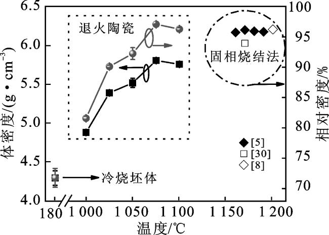
图1 冷烧坯体与退火陶瓷的体密度和相对密度,以及文献[5,8,30]报道的固相烧结法制备陶瓷的相对密度

Fig.1 Bulk densities and relative densities of the cold-sintered pellet and post-annealed ceramics, and the relative densities of the ceramics prepared via the solid-state reaction method reported by references [5,8,30]

2.2 退火温度对试样物相的影响

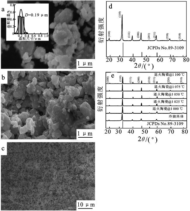
图2a给出前驱粉体的SEM照片及颗粒尺寸统计分布,平均颗粒尺寸约0.19 mm。冷烧坯体和固相烧结法制备的生坯断面SEM分别由图2b2c给出,发现冷烧坯体中晶粒之间已呈现多处紧密结合的晶界,有助于提高其致密性,而固相烧结法压制的生坯中存在大量孔洞,与固相烧结法在室温压制的生坯的相对密度较低的结果相一致。由此可见,冷烧可显著提升坯体的致密性,与其在特定添加液体、适度温度和压力的环境下发生“溶解-沉淀”和塑性形变过程密切相关[22]图2d给出前驱粉体的XRD曲线,其具有纯钙钛矿结构,未观察到第二相。不同温度退火陶瓷的XRD曲线如图2e给出,退火陶瓷均具有纯钙钛矿结构,未观察到与第二相相关的衍射峰,其XRD衍射峰与标准卡片PDF#89-3109吻合[32]
图2 SEM图及XRD曲线

a.前驱粉体SEM图,插图为前驱粉颗粒尺寸分布;b.冷烧坯体断面SEM图;c.固相烧结法制备生坯断面SEM图;d.前驱粉体XRD曲线及JCPDs No. 89-3109标准卡片;e.冷烧坯体和退火陶瓷的XRD曲线。

Fig.2 SEM images and XRD curves

2.3 退火温度对陶瓷显微结构的影响

图3a~e给出不同温度退火陶瓷的SEM图。在1 000 ℃退火的陶瓷中存在较多孔洞,结构不致密,对应其较低的相对密度(~81.6%)。在1 025~1 100 ℃温度退火后,陶瓷的孔洞明显减少,晶界更为清晰,晶粒排列紧密,对应更高的相对密度。由晶粒尺寸分布统计结果(图3f)发现,在1 000 ℃退火陶瓷的平均晶粒尺寸较大(~1.0 mm),当退火温度为1 025~1 100 ℃时平均晶粒尺寸为 0.6~0.8 mm,在宽温区内退火,陶瓷的晶粒尺寸均相近。图3g3h给出1 050 ℃和1 075 ℃退火陶瓷的断面SEM图,可以看出在1 050 ℃退火陶瓷体内存在较多孔洞,陶瓷致密性不佳,其相对密度仅有92.3%;当退火温度升至1 075 ℃时,陶瓷试样体内孔洞显著减少,陶瓷呈现致密的结构。
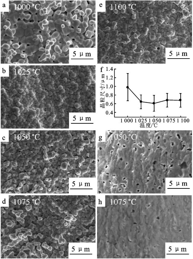
图3 不同温度退火陶瓷的表面SEM图(a~e)和晶粒尺寸统计(f)以及1 050 ℃(g)和1 075 ℃(h)退火陶瓷的断面SEM图

Fig.3 SEM images (a~e) of the ceramics annealed at different temperatures and the statistic of grain sizes(f), and cross-sectional SEM images of the ceramics annealed at 1 050 ℃(g) and 1 075 ℃(h)

2.4 退火温度对陶瓷压电、介电和铁电性能的影响

不同温度退火陶瓷的压电常数d33值如图4所示。在1 025、1 050、1 075和1 100 ℃退火陶瓷的d33值分别为52±7 、95±3 、98±2 和(101±2)pC/N。随退火温度的升高,退火陶瓷的d33值增大。在1 025 ℃退火陶瓷的d33值最低,与其低的相对密度相关(见图1);当退火温度升至1 050 ℃以上时,退火陶瓷的d33值显著升高,其值与固相烧结法制备的BN6BT陶瓷的d33值相当[8]。文献[6]报道了采用固相烧结法在1 160 ℃烧结BN6BT陶瓷,其d33值为125 pC/N,相比之下,本工作中陶瓷的d33值略低,但冷烧并退火方法在较宽的退火温区(1 050~1 100 ℃)获得的陶瓷具有相近的d33值。固相法制备陶瓷的平均晶粒尺寸约1.6 mm[6],本工作中采用冷烧并退火方法制备的陶瓷的平均晶粒尺寸约0.6~0.8 mm。已有研究表明小晶粒具有更多的晶界,对极化过程中畴壁转向的钉扎效应更显著,从而不利于d33提升[33],本工作所得陶瓷的d33值略低,与其具有较小的晶粒尺寸相关。
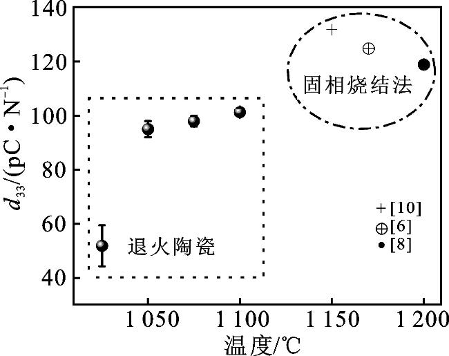
图4 退火陶瓷的d33值和固相烧结法制备的陶瓷的d33值(文献[6,8,10])

Fig.4 The values of d33 for the post-annealed ceramics and the ceramics prepared via the solid-state sintering method(refrence [6,8,10])

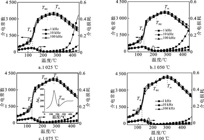
不同温度退火陶瓷经极化后在室温的介电常数εr和介电损耗tan δ值由表1给出。所有退火陶瓷在室温的tan δ≤0.04,εr随退火温度升高而增大。图5给出在不同温度退火陶瓷经极化后的介电温谱。所有陶瓷的介电温谱曲线上呈现3个介电异常特征,其对应的温度分别标记为TRE,TmTd。在常规固相法制备的钛酸铋钠基陶瓷的介电温谱中经常可观察到类似的介电异常特征[8,15]。对TRE介电异常,不同频率的介电常数在TRE温度以下显著不同,当温度高于该温度时,不同频率的介电常数趋于一致。TRE值由Δεr=εr,1 kHz-εr,100 kHz最小值对应的温度确定[5],其中εr,1 kHz表示频率为1 kHz时测试的介电常数,εr,100 kHz表示频率为100 kHz时测试的介电常数。在1 025 、1 050 、1 075和1 100 ℃退火陶瓷的TRE分别是232 、227 、223和220 ℃,TRE随退火温度的增加而减小。
表1 退火陶瓷的介电性能参数

Tab.1 Dielectric properties of the post-annealed ceramics

退火或烧结
温度/℃
εr
(室温)
tan δ
(室温)
Tm/℃ TRE/℃ εm Td/℃ TB/℃ ΔT/℃ γ 文献
1 025 590 0.04 287 232 3 620 130 360 149 1.91 本工作
1 050 604 0.04 284 227 3 616 137 340 198 1.92 本工作
1 075 651 0.03 285 223 3 954 135 350 181 1.85 本工作
1 100 725 0.03 288 220 4 258 123 360 140 1.96 本工作
1 170 740 0.04 273 224 6 266 105 355 81 1.86 [5]
1 200 750 0.03 280 225 5 750 102 413 2 1.90 [8]

注:1 170 ℃和1 200 ℃为烧结温度,陶瓷由固相法制备。

图5 极化陶瓷的介电常数和介电损耗随测试温度变化曲线

c中插图为Δεr随测试温度变化。

Fig.5 Temperature dependence of dielectric constant and dielectric loss of the poled ceramics

标记为Tm的介电异常对应最大介电常数 ε m,对于钛酸铋钠基陶瓷,一般认为Tm值等于居里温度 T c [ 6 ]。在1 025、1 050、1 075和1 100 ℃退火陶瓷的Tm值分别是287、284、285和288 ℃,退火温度对Tm的影响不明显,Tm值与固相烧结法制备的BN6BT陶瓷的相变温度相近(270~290 ℃)[4-8]TRETm处的介电异常通常被认为与陶瓷中极性纳米微区的热演化相关[5-6]
介电损耗曲线在温度Td处出现尖峰,对应的介电常数呈现陡然增大。在钛酸铋钠基陶瓷的介电温谱曲线上该温度常常被用来确定退极化温度[34]。陶瓷试样经极化,其内部的电偶极子总体趋于长程有序状态,随测试温度的升高,长程有序状态逐渐被破坏,当温度大于Td时,陶瓷试样转变为极化前的状态[35-36]。在1 025 、1 050 、1 075和1 100 ℃退火陶瓷的Td值分别为130 、137 、135和123 ℃(见表1)。冷烧并退火制备陶瓷的介电损耗值与固相法制备陶瓷的介电损耗值相近,但介电常数偏低,可能与其具有较小的晶粒尺寸相关。
介电峰在Tm处呈现宽化,表明其具有弥散相变特征。采用居里-外斯定律分析陶瓷的介电弥散特性[37]:
1/εr=(T-T0)/C
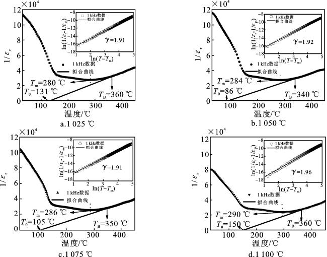
其中:T为测试温度,T0为居里-外斯温度,C为居里-外斯常数,通过拟合数据的截距和斜率分别得到T0C值。图6给出退火陶瓷在1 kHz下1/εr随测试温度的变化曲线。将拟合直线偏离1r随温度变化曲线对应的温度记作玻恩温度TB,其表示在降温过程中,极性纳米微区开始成核的温度[38]TB和ΔT=Tm-T0的数值由表1给出,ΔT均大于0,表明Tm处的相变为一级相变[5]。从不同测试频率得到的介电常数表明:Tm处的介电常数随测试频率变化不显著,TBTm数值存在较大差异,表明弥散相变特征。进一步采用居里-外斯修正定律探究其弥散相变程度[38]:
1/εr-1/εm=(T-Tm)γ/C
其中:γ为弥散系数,其值介于1~2。当γ值等于1时,材料为典型的常规铁电体;γ值等于2时,材料为典型的弛豫铁电体。图6插图给出ln(1/εr-1/εm)随ln(T-Tm)的变化曲线,在1 025、1 050、1 075和1 100 ℃退火陶瓷的γ值分别为1.91、1.92、1.85和1.96。所有陶瓷的γ值均接近2,表明其弥散相变特征。钛酸铋钠基陶瓷的介电弥散相变行为往往与占据同一晶格的不同种类离子和点缺陷因素相关[4,39]
图6 退火陶瓷1/ ε r随温度变化曲线

插图给出ln(1/εr-1/εm)随ln(T-Tm)的变化,实线为居里-外斯修正拟合曲线。

Fig.6 The relationship of 1/ ε r and T for the post-annealed ceramics annealed

不同温度退火陶瓷的电滞回线如图7所示,测试频率为1 Hz,测试电压为40~100 kV/cm。对给定样品,随测试电压增大,电滞回线趋于饱和,在最大测试电压下所得电滞回线呈现典型的铁电体回线特征。对给定温度退火的陶瓷,随测试电压增大,最大极化强度Pm、剩余极化强度Pr和矫顽场Ec逐渐增大。在测试电压100 kV/cm下,在1 075 ℃退火的陶瓷具有最高的极化强度值,PmPr分别为60.9 mC/cm2和51.8 mC/cm2。用曲线方形因子Rsq表征铁电性[40]:
Rsq=(Pr/Ps)+(P1.1Ec/Pr)。
其中:Ps表示饱和极化强度;P1.1Ec表示测试电场为1.1倍的Ec时对应的极化强度。对于理想的方形回路,Rsq=2。测试电压100 kV/cm时,在1 025、1 050、1 075和1 100 ℃退火陶瓷的Rsq值分别为2.0、2.1、1.9和2.0,表明其良好的铁电性能。
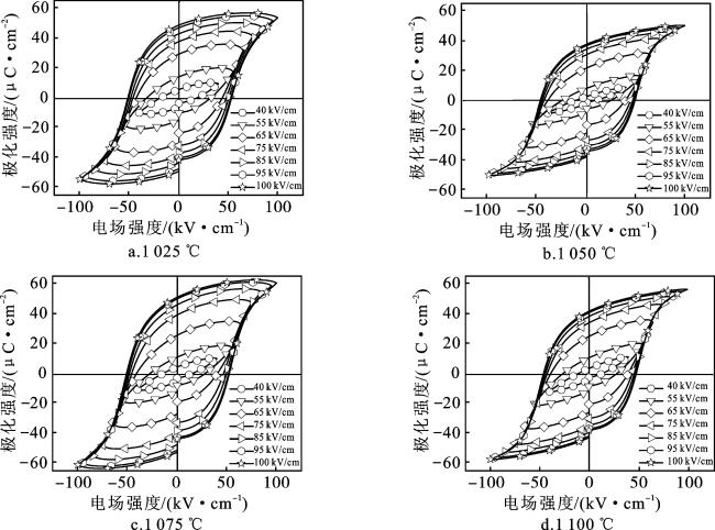
图7 退火陶瓷的电滞回线

Fig.7 P-E loops of the ceramics annealed at different temperatures

将本研究中冷烧并退火制备陶瓷的电学性能参数PmPrEcTdd33值与固相烧结法制备陶瓷的性能参数值进行了对比,如图8所示。固相烧结法制备致密BN6BT陶瓷的烧结温度为1 170 ℃,其在75 kV/cm下测量的PmPrTd值分别为40.4 C/cm2、34.3 C/cm2和105 ℃[6];冷烧并在1 075 ℃退火陶瓷对应的PmPrTd值分别为60.9 C/cm2、51.8 C/cm2和135 ℃,后者呈现更高的极化强度和退极化温度,表现出良好的铁电和介电性能。相较于固相烧结法制备的陶瓷,冷烧并退火陶瓷的d33值略低,但仍接近100 pC/N。此外,使用耐压仪测试直流电下陶瓷的击穿场强(breakdown strength,BDS),在1 025、1 050、1 075和1 100 ℃退火陶瓷的BDS分别为153、150、157和152 kV/cm。冷烧并退火陶瓷的击穿场强均大于100 kV/cm,该值高于采用固相烧结法制备的具有相同组成陶瓷的BDS(<75 kV/cm)[10,12,41]。采用冷烧并退火方法,将获得致密BN6BT陶瓷的处理温度降到1 100 ℃及以下,远低于固相法制备BN6BT陶瓷的烧结温度(1 160 ℃) [6]。较低的处理温度,有利于降低阳离子挥发,且所制备陶瓷的晶粒尺寸显著降低,有利于提高其BDS[42]。由此可见,相较于固相烧结法,冷烧并退火工艺在有效降低制备温度的同时能保持陶瓷试样良好的致密性和电学性能。
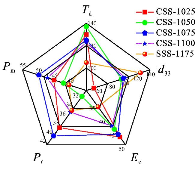
图8 冷烧并退火方法(简称CSS)与传统固相法(简称SSS)制备BN6BT陶瓷的性能参数对比

注:网络版为彩图。

Fig.8 Comparison of the electrical properties of the ceramics via CSS and SSS

3 结论

本研究采用冷烧并退火方法制备了BN6BT陶瓷,研究了退火温度对陶瓷试样的物相组成、显微组织、介电、铁电和压电性能等的影响。所有退火陶瓷均为纯钙钛矿结构。随着退火温度的升高,陶瓷的相对密度先增加后降低,在1 075 ℃退火陶瓷的相对密度最高为97.1%。在1 025~1 100 ℃退火陶瓷的平均晶粒尺寸为600~800 nm。极化陶瓷的介电温谱曲线上呈现3个介电异常特征。退火陶瓷在Tm处均呈现弥散相变特征,弥散相变因子接近2。所有退火陶瓷的BDS均大于100 kV/cm,在1 075 ℃退火陶瓷呈现良好的电学性能,其中PmPrTdd33分别为60.9 C/cm2、51.8 C/cm2、135 ℃和(98±2) pC/N。结果表明,相较于固相烧结法,冷烧并退火方法制备钛酸铋钠基陶瓷能在有效降低处理温度的同时保持陶瓷良好的电学性能,本研究为采用冷烧结技术制备其他钙钛矿结构的压铁电体陶瓷提供了参考。
[1]
SHI W J, ZHANG L Y, JING R Y, et al. Relaxor antiferroelectric-like characteristic boosting enhanced energy storage performance in eco-friendly (Bi0.5Na0.5)TiO3-based ceramics[J]. Journal of the European Ceramic Society, 2022, 42(11):4528-4538.

DOI

[2]
WANG X Y, LIU X Y, XUE H Y, et al. Temperature-independent large strain with small hysteresis in Sb-modified BNT-based lead-free ceramics[J]. Journal of the American Ceramic Society, 2022, 105(3):2116-2127.

DOI

[3]
LIU L N, CHEN X M, JING R Y, et al.Comparative study on (Na0.47Bi0.47Ba0.06)0.95A0.05TiO3 (A = Sr2+/ Ca2+) lead-free ceramics: scaling behavior of ferroelectric hysteresis loop[J]. Applied Physics Letters, 2022, 120(2): 022902.

DOI

[4]
陈晓明, 刘丽娜, 王星星, 等. (Na0.5Bi0.5)0.94Ba0.06TiO3陶瓷的结构及电学性能:点缺陷效应研究进展[J]. 陕西师范大学学报(自然科学版), 2021, 49(4):2-29.

CHEN X M, LIU L N, WANG X X, et al. An overview of structure and electrical properties of (Na0.5Bi0.5)0.94Ba0.06TiO3 ceramics:point defects effect[J]. Journal of Shaanxi Normal University (Natural Science Edition), 2021, 49(4):2-29.

[5]
QIAO X S, CHEN X M, LIAN H L, et al. Dielectric,ferroelectric,piezoelectric properties and impedance analysis of nonstoichiometric (Bi0.5Na0.5)0.94+xBa0.06TiO3 ceramics[J]. Journal of the European Ceramic Society, 2016, 36(16):3995-4001.

DOI

[6]
QIAO X S, CHEN X M, LIAN H L, et al. Microstructure and electrical properties of nonstoichiometric 0.94(Na0.5Bi0.5+x)TiO3-0.06BaTiO3 lead-free ceramics[J]. Journal of the American Ceramic Society, 2016, 99(1):198-205.

DOI

[7]
连汉丽, 王若晨, 石锦延, 等. Bi0.44Na0.50Ba0.06TiO3-δ与Bi0.50Na0.44Ba0.06TiO3+δ无铅陶瓷的显微结构、 介电及铁电性能[J]. 陕西师范大学学报(自然科学版), 2021, 49(4):69-78.

LIAN H L, WANG R C, SHI J Y, et al.Microstructure, dielectric and ferroelectric properties of Bi0.44Na0.50Ba0.06TiO3-δ and Bi0.50Na0.44Ba0.06TiO3+δ lead-free ceramics[J]. Journal of Shaanxi Normal University (Natural Science Edition), 2021, 49(4):69-78.

[8]
LIAN H L, SHAO X J, CHEN X M. Structure and electrical properties of Ca2+-doped (Na0.47Bi0.47Ba0.06)TiO3 lead-free piezoelectric ceramics[J]. Ceramics International, 2018, 44(10):11320-11330.

DOI

[9]
ZHANG Y, FU J, XIE A W, et al. NaNbO3 modulated phase transition behavior and antiferroelectric stability evolution in 0.88(Bi0.5Na0.5)TiO3-0.12BaTiO3 lead-free ceramics[J]. Journal of Materiomics, 2022, 8(5):1067-1076.

DOI

[10]
LIU L N, CHEN X M, JING R Y, et al. Electrical and photoluminescence properties of (Bi0.5-x/0.94Erx/0.94Na0.5)0.94Ba0.06TiO3 lead-free ceramics[J]. Journal of Materials Science:Materials in Electronics, 2019, 30(5):5233-5239.

DOI

[11]
张文婷, 景瑞轶, 陈晓明. 氮气、 氧气烧结气氛对(Na0.5Bi0.5)0.94Ba0.06TiO3陶瓷显微结构和电学性能的影响[J]. 陕西师范大学学报(自然科学版), 2017, 45(2):29-35.

ZHANG W T, JING R Y, CHEN X M. Effects of nitrogen and oxygen atmospheres at calcination and sintering processes on microstructure and electrical properties of (Na0.5Bi0.5)0.94Ba0.06TiO3 ceramics[J]. Journal of Shaanxi Normal University (Natural Science Edition), 2017, 45(2):29-35.

[12]
LIAN H L, SHAO X J, CHENG R X. Improved ferroelectric and piezoelectric properties of (Na0.47Bi0.47Ba0.06)0.97Sr0.03TiO3 lead-free ceramics sintered in nitrogen atmosphere[J]. Ferroelectrics, 2020, 555(1):161-172.

DOI

[13]
LIAN H L, CHENG R X, SHI J Y. Ferroelectric and dielectric properties of (Na0.47Bi0.47Ba0.06)0.99Ca0.01TiO3 ceramics sintered in different atmospheres[J]. Phase Transitions, 2020, 93(2):236-244.

DOI

[14]
CHEN X M, PAN W Y, TIAN H H, et al.Microstructure, dielectric and ferroelectric properties of 0.94Bi0.5Na0.5TiO3-0.06BaTiO3 (NBTB) and 0.05BiFeO3-0.95NBTB ceramics:effect of sintering atmosphere[J]. Journal of Alloys and Compounds, 2011, 509(5):1824-1829.

DOI

[15]
MA J P, CHEN X M, LIAN H L, et al.Microstructure, dielectric,piezoelectric,and ferroelectric properties of fine-grained 0.94Na0.5Bi0.5TiO3-0.06BaTiO3 ceramics[J]. Journal of the European Ceramic Society, 2019, 39(2/3):264-268.

DOI

[16]
FANCHER C M, JO W, RÖDEL J, et al. Effect of texture on temperature-dependent properties of K0.5Na0.5NbO3 modified Bi1/2Na1/2TiO3-xBaTiO3[J]. Journal of the American Ceramic Society, 2014, 97(8):2557-2563.

DOI

[17]
HAO J G, YE C G, SHEN B, et al. Enhanced electrostricitive properties and thermal endurance of textured (Bi0.5Na0.5)TiO3-BaTiO3-(K0.5Na0.5)NbO3 ceramics[J]. Journal of Applied Physics, 2013, 114(5):054101.

DOI

[18]
LI Z T, LIU H, THONG H C, et al. Enhanced temperature stability and defect mechanism of BNT-based lead-free piezoceramics investigated by a quenching process[J]. Advanced Electronic Materials, 2019, 5(3):1800756.

DOI

[19]
QIU Y Z, CHEN X M, LIAN H L, et al. Structure and electrical behavior of unpoled and poled 0.97(Bi0.5Na0.5)0.94Ba0.06TiO3-0.03BiAlO3 ceramics[J]. Materials Chemistry and Physics, 2017, 202:197-203.

DOI

[20]
GUO J, GUO H Z, BAKER A L, et al. Cold sintering:a paradigm shift for processing and integration of ceramics[J]. Angewandte Chemie International Edition, 2016, 55(38):11457-11461.

DOI

[21]
GUO H Z, BAKER A, GUO J, et al. Cold sintering process:a novel technique for low-temperature ceramic processing of ferroelectrics[J]. Journal of the American Ceramic Society, 2016, 99(11):3489-3507.

DOI

[22]
付长利, 李晓萌, 郭靖. 基于冷烧结技术的电介质材料研究进展[J]. 陕西师范大学学报(自然科学版), 2021, 49(4):30-42.

FU C L, LI X M, GUO J. Recent progress of dielectric materials prepared via cold sintering process[J]. Journal of Shaanxi Normal University (Natural Science Edition), 2021, 49(4):30-42.

[23]
WANG D W, LI L H, JIANG J, et al. Cold sintering of microwave dielectric ceramics and devices[J]. Journal of Materials Research, 2021, 36(2):333-349.

DOI

[24]
JIA Y Q, HONG W B, LI L, et al. Dense LiF microwave dielectric ceramics with near-zero linear shrinkage during sintering[J]. Ceramics International, 2022, 48(19):28463-28470.

DOI

[25]
GUO H Z, GUO J, BAKER A, et al. Hydrothermal-assisted cold sintering process:a new guidance for low-temperature ceramic sintering[J]. ACS Applied Materials & Interfaces, 2016, 8(32):20909-20915.

[26]
MA J P, CHEN X M, OUYANG W Q, et al.Microstructure, dielectric, and energy storage properties of BaTiO3 ceramics prepared via cold sintering[J]. Ceramics International, 2018, 44(4):4436-4441.

DOI

[27]
HUANG H Q, TANG J, LIU J. Preparation of Na0.5Bi0.5TiO3 ceramics by hydrothermal-assisted cold sintering[J]. Ceramics International, 2019, 45(6):6753-6758.

DOI

[28]
李冰玉, 刘美丹, 兰佳俊, 等. K0.5Na0.5NbO3陶瓷的冷烧及其介电与铁电性能[J]. 陕西师范大学学报(自然科学版), 2021, 49(4):96-105.

LI B Y, LIU M D, LAN J J, et al. Cold sintering K0.5Na0.5NbO3 ceramics and their dielectric,ferroelectric properties[J]. Journal of Shaanxi Normal University (Natural Science Edition), 2021, 49(4):96-105.

[29]
LAN J J, CHEN X M, LIU L N, et al. Low-temperature synthesis of K0.5Na0.5NbO3 ceramics in a wide temperature window via cold-sintering assisted sintering method and enhanced electrical properties[J]. Journal of the European Ceramic Society, 2023, 43(1):73-81.

DOI

[30]
CHEN X M, GONG X X, LI T N, et al.Microstructure, dielectric and ferroelectric properties of (1-x)(0.94Bi0.5Na0.5TiO3-0.06BaTiO3)-xBiFeO3 lead-free ceramics synthesized via a high energy ball milling method[J]. Journal of Alloys and Compounds, 2010, 507(2):535-541.

DOI

[31]
POLOTAI A, BREECE K, DICKEY E, et al. A novel approach to sintering nanocrystalline barium titanate ceramics[J]. Journal of the American Ceramic Society, 2005, 88(11):3008-3012.

DOI

[32]
International Center for Diffraction Data ICDD. PDF-2: #89-3109[DB/OL]. [2022-12-05]. http://icddchina.com/pdf2.html.

[33]
MARTIRENA H T, BURFOOT J C. Grain-size effects on properties of some ferroelectric ceramics[J]. Journal of Physics C:Solid State Physics, 1974, 7(17):3182-3192.

DOI

[34]
HAO J G, XU Z J, CHU R Q, et al. Structure evolution and electrostrictive properties in (Bi0.5Na0.5)0.94Ba0.06TiO3-M2O5 (M=Nb,Ta,Sb) lead-free piezoceramics[J]. Journal of the European Ceramic Society, 2016, 36(16):4003-4014.

DOI

[35]
ANTON E M, JO W, DAMJANOVIC D, et al. Determination of depolarization temperature of (Bi1/2Na1/2)TiO3 based lead-free piezoceramics[J]. Journal of Applied Physics, 2011, 110(9):094108.

DOI

[36]
MALIK R A, HUSSAIN A, MAQBOOL A, et al. Temperature-insensitive high strain in lead-free Bi0.5(Na0.84K0.16)0.5TiO3-0.04SrTiO3 ceramics for actuator applications[J]. Journal of the American Ceramic Society, 2015, 98(12):3842-3848.

DOI

[37]
BOKOV A A, YE Z G. Recent progress in relaxor ferroelectrics with perovskite structure[J]. Journal of Materials Science, 2006, 41(1):31-52.

DOI

[38]
UCHINO K, NOMURA S. Critical exponents of the dielectric constants in diffused-phase-transition crystals[J]. Ferroelectrics, 1982, 44(1):55-61.

DOI

[39]
XU Q, HUANG D P, CHEN M, et al. Effect of bismuth excess on ferroelectric and piezoelectric properties of a (Na0.5Bi0.5)TiO3-BaTiO3 composition near the morphotropic phase boundary[J]. Journal of Alloys and Compounds, 2009, 471(1/2):310-316.

DOI

[40]
HARETLING G H, ZIMMER W J. Analysis of hot pressing parameters for lead-zirconate-lead titanate ceramics containing two atom percent bismuth[J]. American Ceramic Society Bulletin, 1996, 45(12) 1084-1087.

[41]
MA H Y, CHEN X M, WANG J, et al.Structure, dielectric and ferroelectric properties of 0.92Na0.5Bi0.5TiO3-0.06BaTiO3-0.02K0.5Na0.5NbO3 lead-free ceramics:effect of Co2O3 additive[J]. Ceramics International, 2013, 39(4):3721-3729.

DOI

[42]
FENG Q, LIU X Y, CHEN G H, et al. Dielectric,ferroelectric and energy storage properties of (1-x) Bi0.47Na0.47Ba0.06TiO3-xBaZrO3 glass ceramics[J]. Journal of Materials Science:Materials in Electronics, 2016, 27(6):6282-6291.

DOI

Outlines

/